But GSM antennas are what makes it possible for our phones to work properly, identical to Signal's product rf coaxial cable. They work by using radio communications to establish a call between our phone and the mobile network. A GSM antenna PCB when in perfect shape will significantly increase the chances of our connection remaining stable and constantometrics/pedalino.
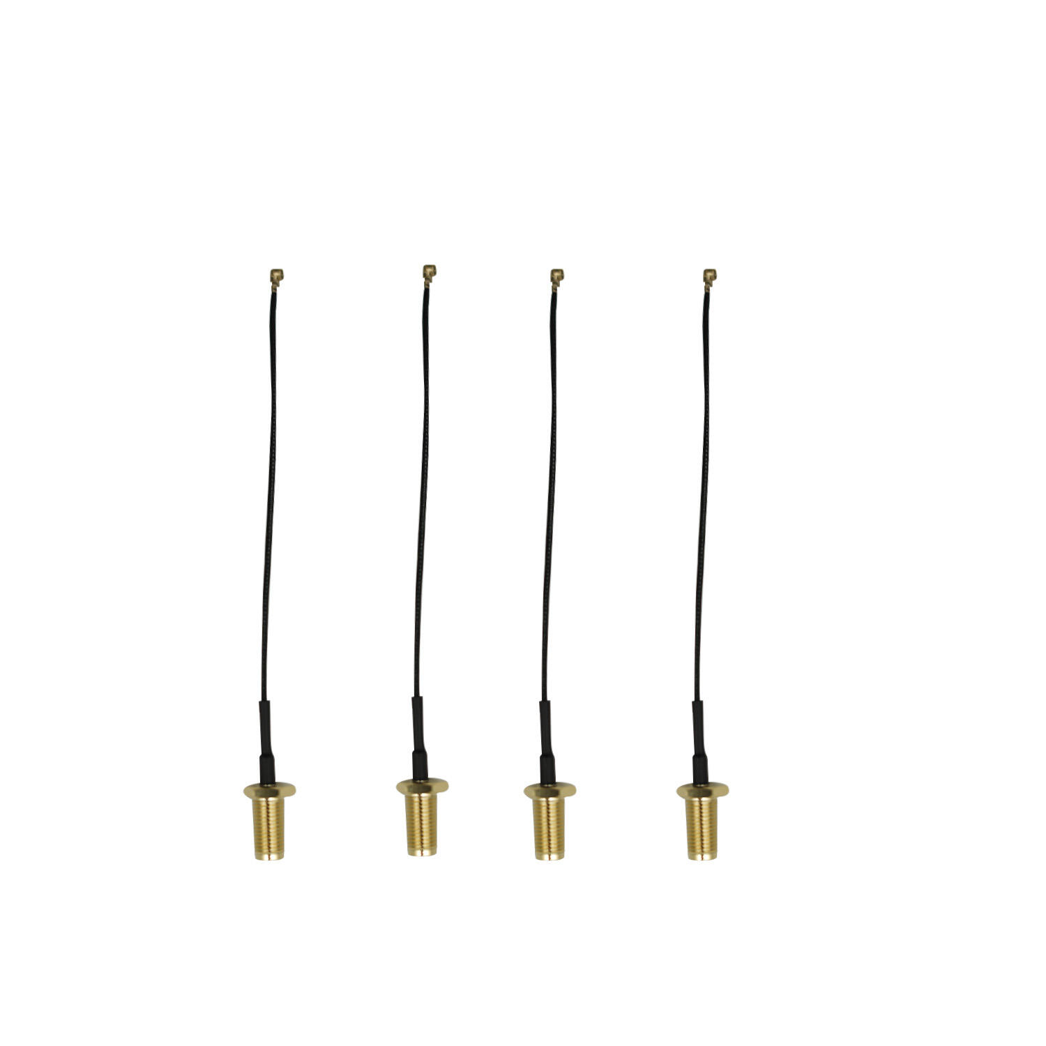
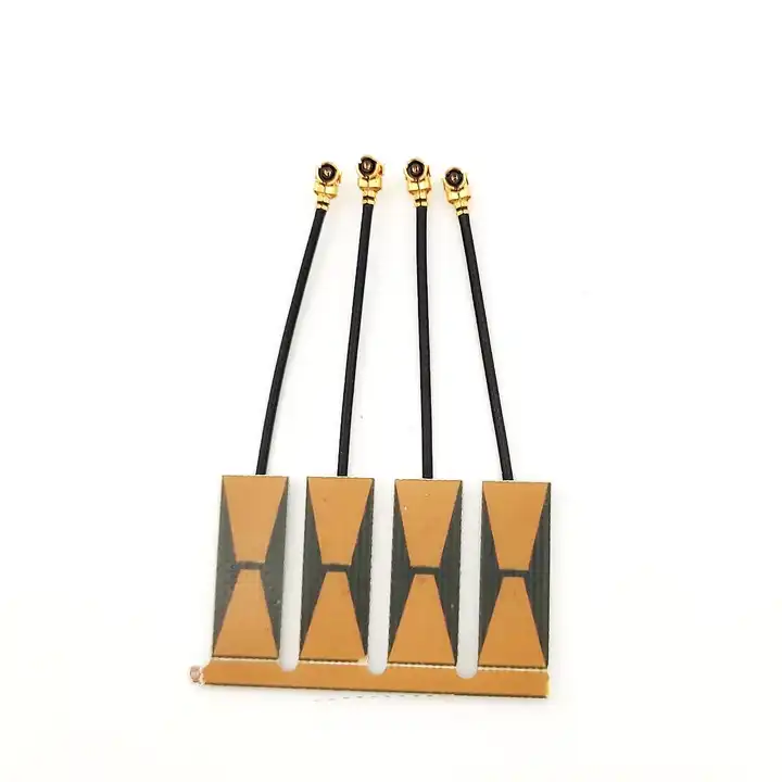
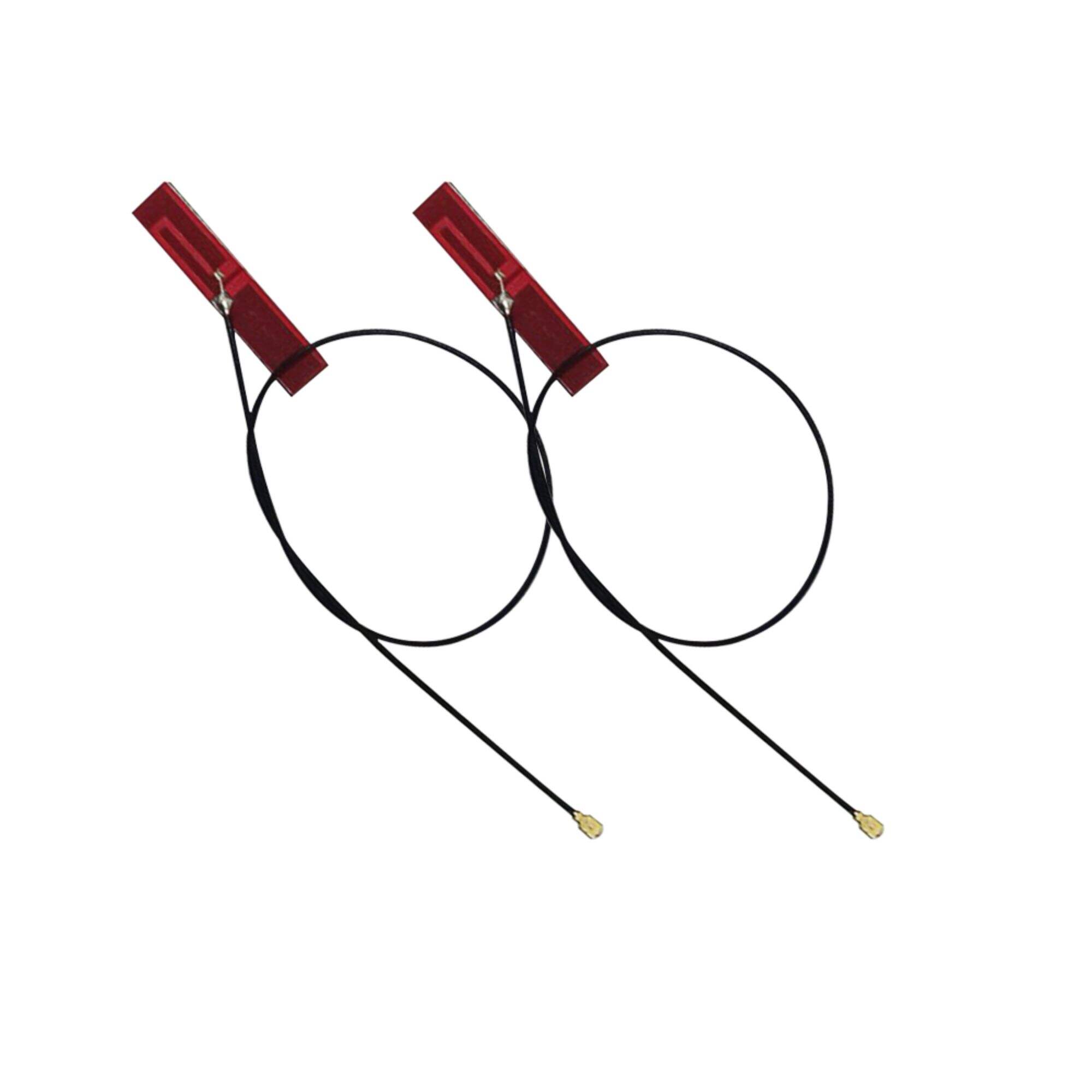
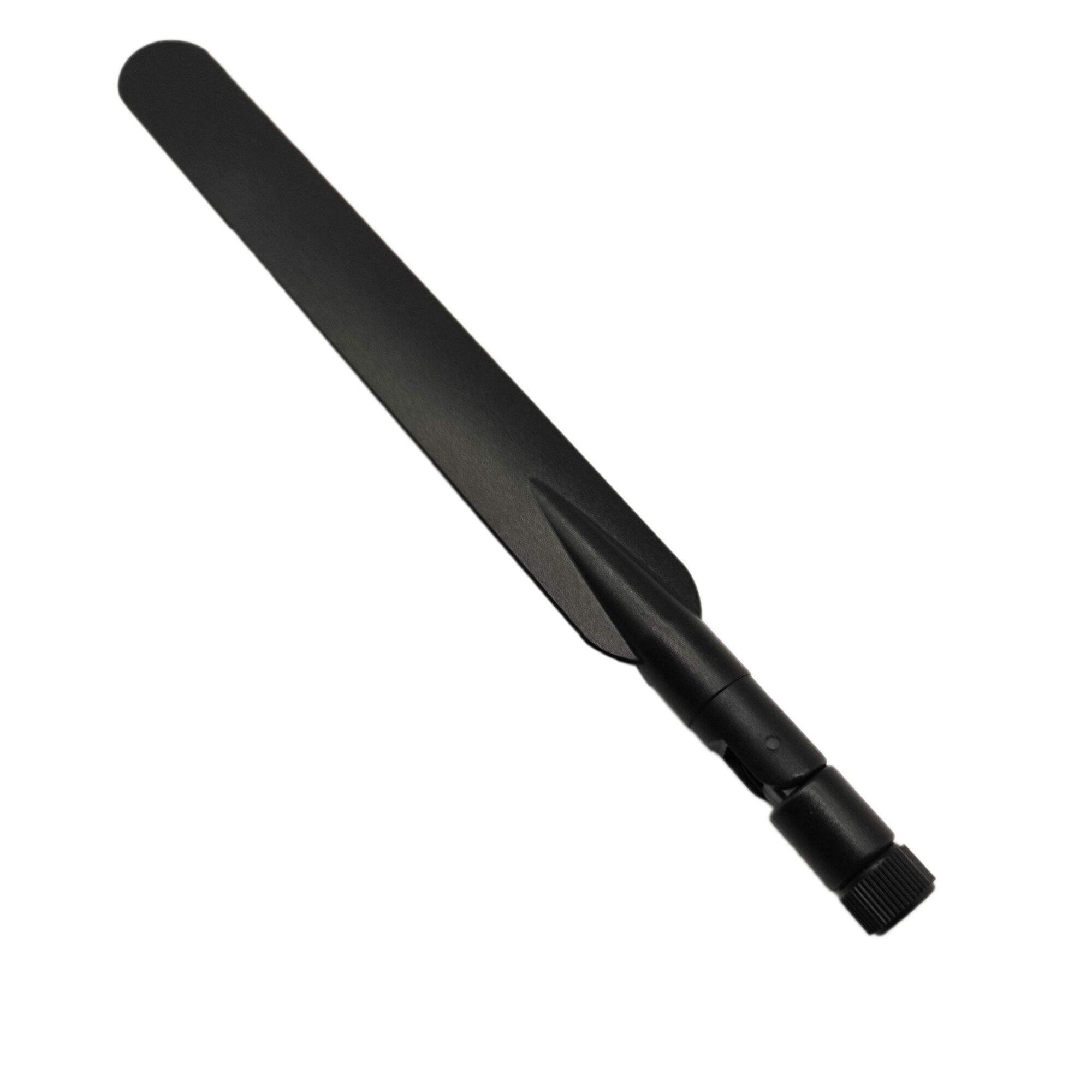
A GSM antenna PCB, a printed circuit board is an essential ingredient in setting and tuning the signal through a GSM antenna, also the long range wifi receiver antenna by Signal. A PCB design with GSM antenna must consider the size of the trace, board parameters like geometry and component placement. Designing a superior PCB results in an antenna with performance assured, so that the work reliability and efficiency of it is ensured.
Importance of a Good Quality PCB Layout in Durable GSM Antenna
One of the essential factors responsible for guaranteeing a reliable performance GSM antenna is its PCB layout. With careful placement of components on the board to have a well-connected defined system, we can reduce the risk of hindering radiated efficiency by other elements than just that antenna itself. In other words, a good GSM antenna is one that can both emit and receive signals adequately over long distances in harsh terrains.
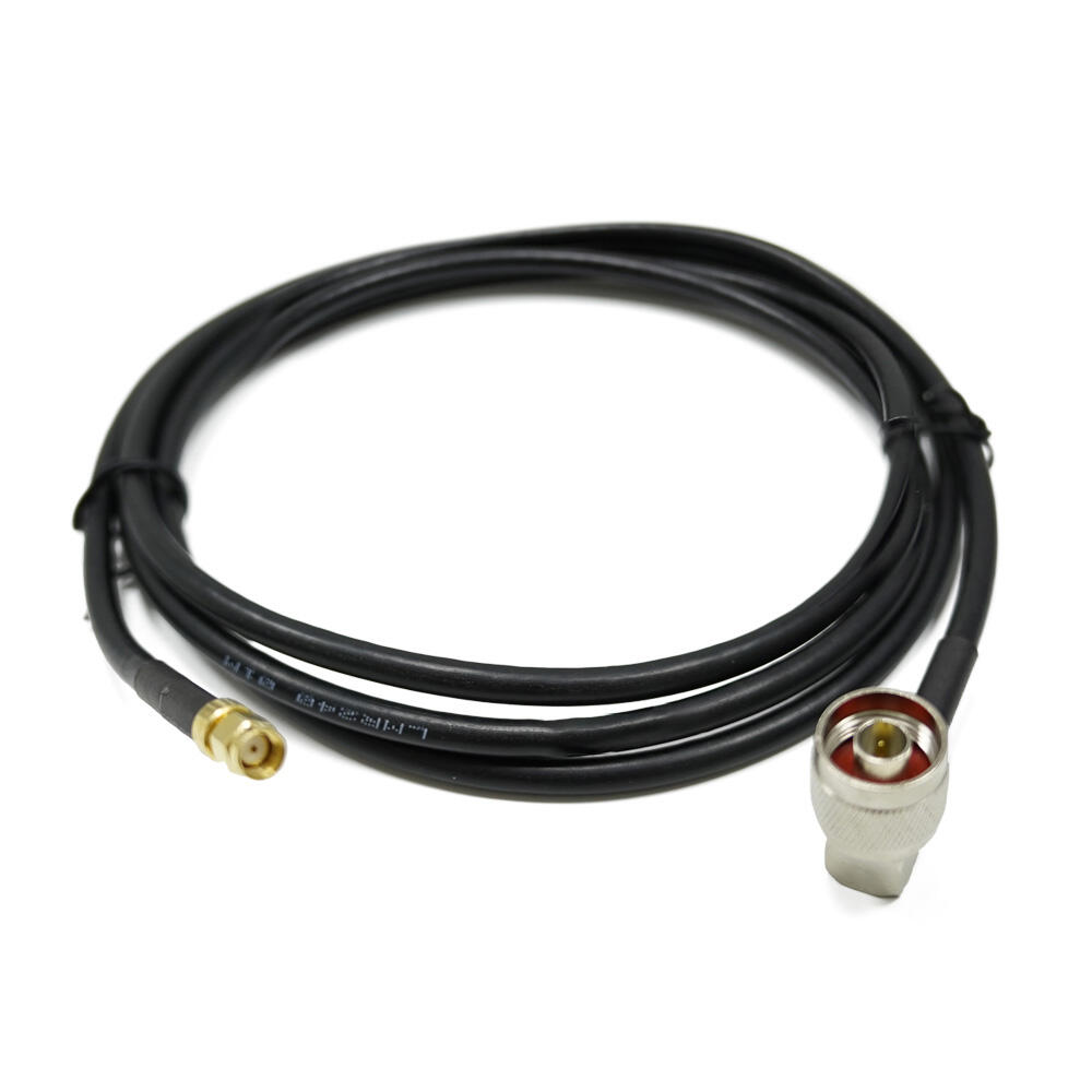
Even when we do our best GSM antennas on PCBs can be problematic, identical to Signal's product male to male rf cable. Problems include a weak or low-quality signal, electrical noise from other devices and even damage to the antenna. These are amongst everything else which causes problems with your GSM antenna and you may need to debug the cause. Most of the time, this means checking out antenna wiring and connector details or tweaking PCB layout if required.
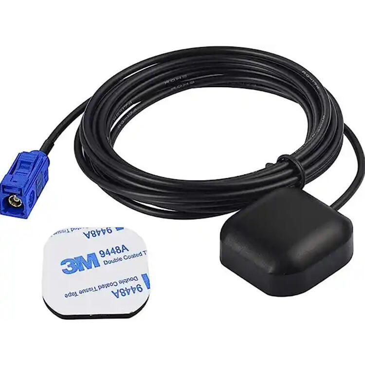
Having a high-quality GSM antenna PCB will greatly enhance your network reception and in turn the performance of cell phone or devices using it, similar to the outdoor gps antenna supplied by Signal. With an optimized antenna performance, which features high quality design and reliability you will still get a strong signal that works flawlessly even in harsh environments. No matter how you use your phone, a good network connection is crucial for keeping in touch with family and friends as well providing efficient work capabilities.
Here are some of the effective strategies for positioning your GSM antenna on a PCB.
There are numerous best practices to follow when siting a GSM antenna on PCB. These rules can range from choosing the right size and shape of your antenna to placing it at a proper location in circuit board, using materials that may have durability for long run. ConclusionWith the above best practices, you can guarantee proper performance of your antenna making them reliable and efficient.
One of the most critical aspects in our mobile technology are GSM antennas, which connects us with everything that lays around, identical to Signal's product antenna wifi bluetooth. The use of a highly soldered GSM antenna PCB helps maximize the performance of the antennae, therefore guaranteeing that you will always be receiving strong signals in any work scenario. If we follow best practices and correct any issues that may arise quickly, it is possible to achieve full connectivity 24/7 wherever you are situated.
Signal Plus Gsm antenna pcb years manufacturing experience LTE antenna,GPS antenna industry.Annual shipment quantity reaches 20,000,000 antenna units.Company 450+employees production 20 Lines meet customers'requirements full terms.
Gsm antenna pcb a top supplier antennas support 2G/3G/4G/5G, WIFl antenna, Lora, GPS, FPC/PCB, Combo, Fiberglass more. 9000 square meters facility a rich RD team, Signal Technology Co. Ltd established 2015.
Gsm antenna pcb 20 structural engineers Engineers RF 285 production personnel 10,000 SM factory. 62 patents communications antennas GPS antennas. than 100 countries regions are served.
provide simulation services Gsm antenna pcb HFSS software provide simulation services HFSS software.

 EN
EN
 ES
ES
 PT
PT
 NL
NL
 AR
AR
 HR
HR
 CS
CS
 DA
DA
 FI
FI
 FR
FR
 DE
DE
 EL
EL
 IT
IT
 JA
JA
 KO
KO
 NO
NO
 PL
PL
 RO
RO
 RU
RU
 SV
SV
 TL
TL
 IW
IW
 ID
ID
 LT
LT
 SR
SR
 SK
SK
 SL
SL
 UK
UK
 VI
VI
 ET
ET
 HU
HU
 MT
MT
 TH
TH
 TR
TR
 FA
FA
 GA
GA
 BE
BE
 IS
IS
 LB
LB
 BG
BG