When it comes to technology, we always wonder what different parts come together in creating something that is considered smart. A standout component to mention is the NFC antenna PCB. This tiny but powerful technology plays a significant role in the flawless operation of our daily devices. In this article, we will be discussing NFC antenna PCBs and how they are integral to developing various smart devices. We also cover the detail on how to design efficient NFC antenna PCBs for different applications, secure data transfer technology and potential of NFC Antenna PCB in many IoT (Internet of Things) based application cases.
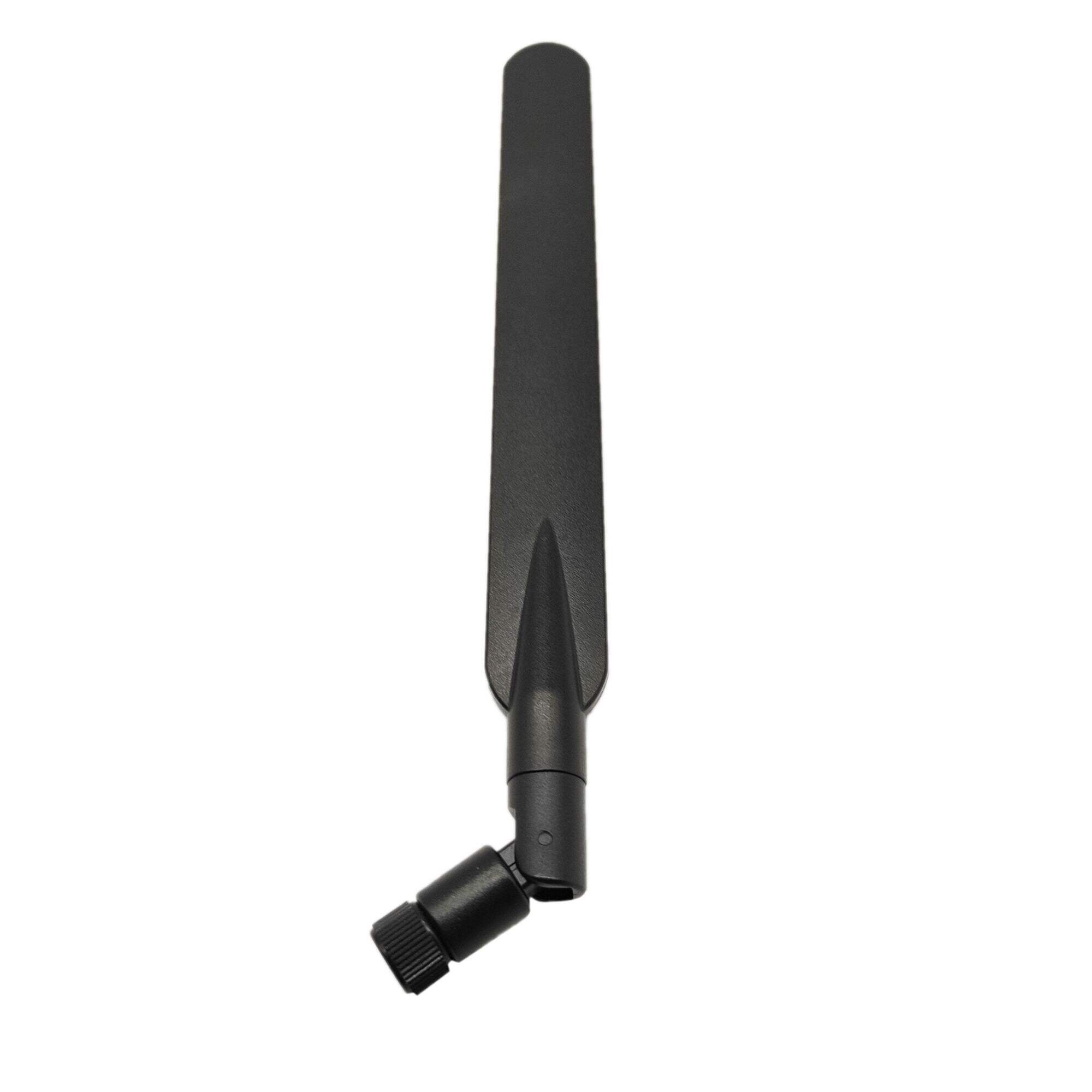
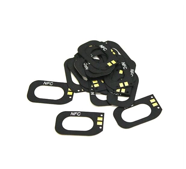
NFC (Near Field Communication!...) is a brilliant technology for phones, which allows devices to communicate at short range. A hidden gem within our smart gadgets, the NFC antenna PCB (as you can imagine, a tiny circuit board that we do not see) was built into them specifically to enable such communication. These devices function by creating a magnetic field that can communicate with other nearby NFC-compatible equipment.
NFC technology in everyday devices has seen a rise, from smartphones to smart home appliances. The popularity has increased by leaps and bounds because of its conveniency in terms of transferring data within seconds, without any cords or third party setups.
Deciphering the Role of NFC Antenna PCB in Smart Device Development
NFC antenna PCBs deserve more attention in the era of smart devices. The tiny PCBs play the part of a bridge for devices to send data across smooth, fast and safe in use. NFC-enabled devices can connect to each other quickly, and you will be able to share data like contacts or multimedia files with others as well as reading the information on digital posters.
They form an integral part of the production process for myriad smart devices including payment systems, door locks and medical tools using NFC antenna PCBs. These PCBs also help for Tap and pay in retail environments such that Payments made quickly contactless with NFC mobile handsets.
However, the development of efficient NFC antenna PCBs needs to see designers follow certain strategies. While it is essential to use high-quality materials and place components strategically. In addition, issues like board dimensions or form factor and power consumption play a big role when optimal performance is desired.
Designers must consider the antenna design and matching circuits outside of ensuring top-performance NFC antennae PCBs for a myriad of applications. Where the aerial design has a major influence on not only how wide of an area and range in which the PCB will produce its current magnetc field, but also that ensures for any given operational mode (e.g. reading /writing data) to function correctly with maximum signal strength via matching circuits.
NFC, the cutting edge technology is used for smooth data transfer and safe transaction. One can use NFC enabled devices to send data or make payments in a controlled environment, without revealing his personal information.
One of the key advancements in NFC technology is secure elements. These dedicated chips that are integrated within the NFC antenna PCB secure sensitive information, such as payment details protecting it from unauthorised access and theft.
Internet of Things (IoT) is an emerging area which basically hooks up everyday devices and sensors to the web. In IoT, NFC Antenna PCBs for communication and data exchange across devices is the mainstay.
NFC antenna PCBs are highly diverse in the realm of IoT, and cover applications from home automation to healthcare. These PCBs are then embedded in sensors, which transforms it into a smart device that can be controlled and monitored from anywhere home or business. Moreover, NFC antenna PCBs can be used for remote monitoring and quick diagnostics in healthcare.
When we sum up, we can say that NFC antenna PCBs play an essential role within smart devices to transmit data in a secure and time-efficient manner. For different applications, there are stringent design strategies that designers must follow in order to realise effective NFC antenna PCBs and troubleshoot related problems-made possible by cutting-edge technology for seamless data transfer. NFC antenna PCBs for IoT have the potential to contribute quite some enrichments in our lives like improved convenience, comfort and security.
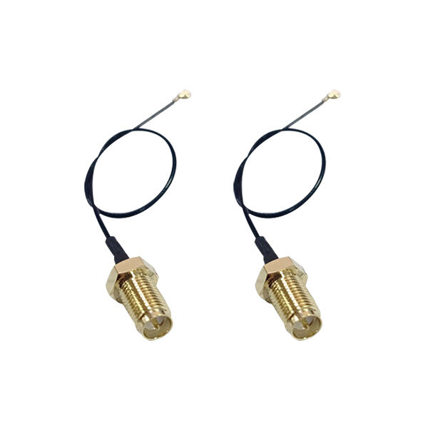
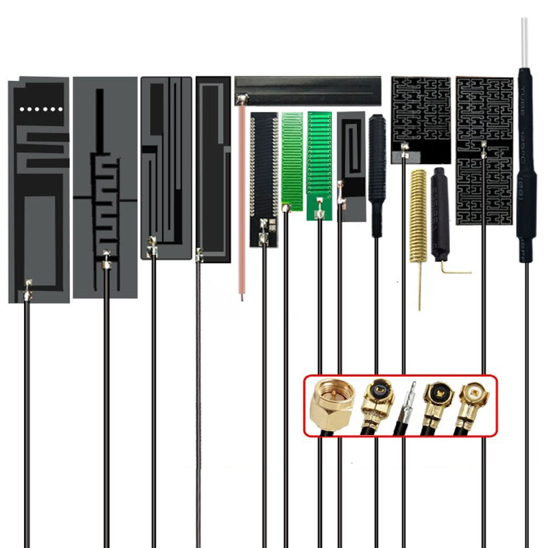
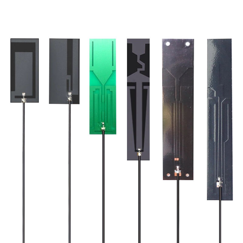
products designed manufactured strictly accordance ISO9001SO14001, ROHS REACH any custom made antenna, nfc antenna pcb project supported offer simulations use HFSS software.
Signal Plus Technology Co, Ltd. a leading manufacturer antennas 2G/3G/4G/5G, WIFlantenna, nfc antenna pcb, GPS FPC/PCB, Combo Fiberglass, etc. Since inception 2015 9000 square meter factory rich experienced RD team.
nfc antenna pcb 20 structural engineers well as engineers RF 285 production personnel 10,000 SM factory. Company 62 patents communications antennas as well GPS antennas. 100 countries areas served.
Signal Plus 10 years manufacturing experience LTE antenna, GPS antenna industry. Annual shipment quantity reaches nfc antenna pcb antenna units. Company has 450+employees and production 20 Lines that meet all customers' requirements full terms.

 EN
EN
 ES
ES
 PT
PT
 NL
NL
 AR
AR
 HR
HR
 CS
CS
 DA
DA
 FI
FI
 FR
FR
 DE
DE
 EL
EL
 IT
IT
 JA
JA
 KO
KO
 NO
NO
 PL
PL
 RO
RO
 RU
RU
 SV
SV
 TL
TL
 IW
IW
 ID
ID
 LT
LT
 SR
SR
 SK
SK
 SL
SL
 UK
UK
 VI
VI
 ET
ET
 HU
HU
 MT
MT
 TH
TH
 TR
TR
 FA
FA
 GA
GA
 BE
BE
 IS
IS
 LB
LB
 BG
BG