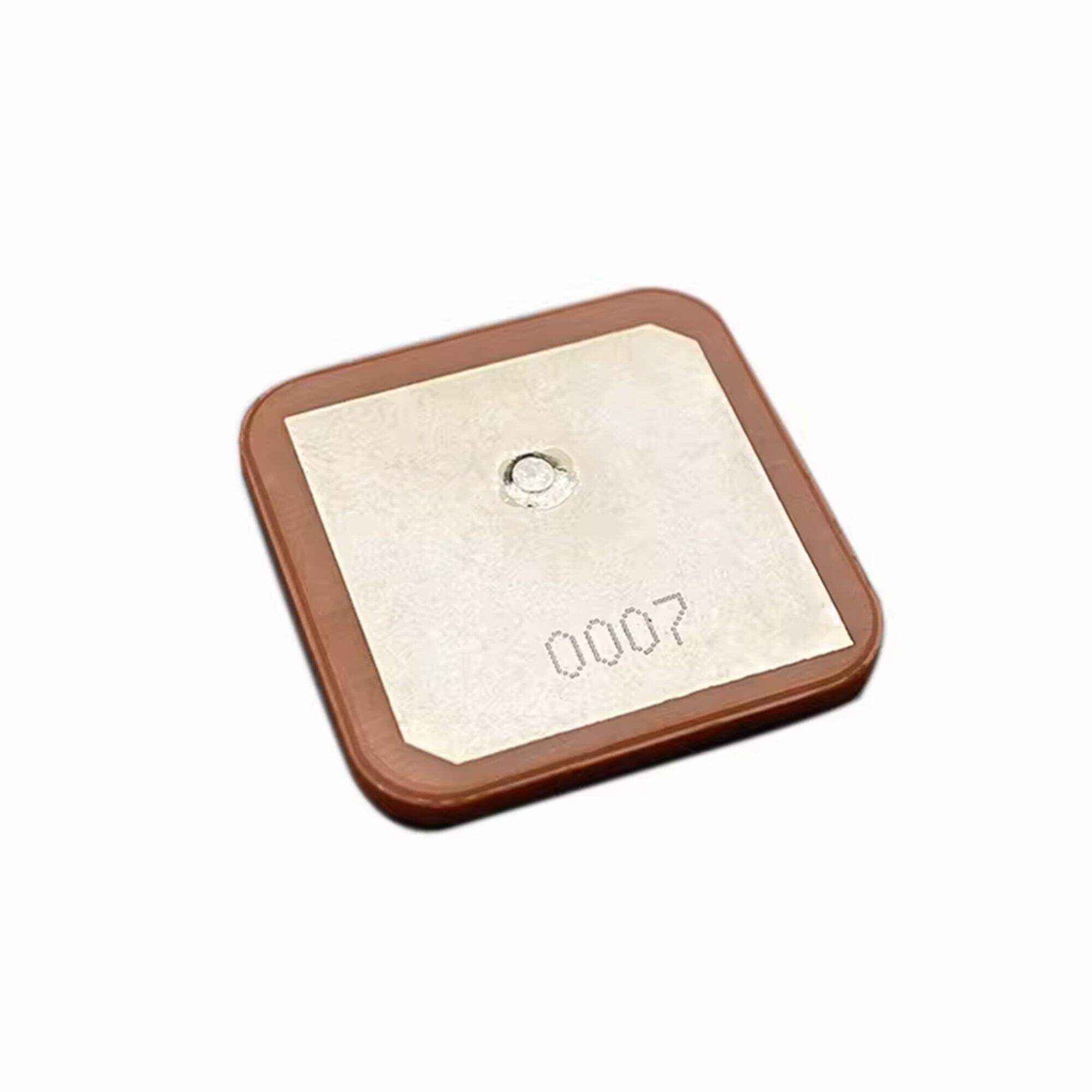
What are NFC antenna PCBs? NFC antenna PCBs are Minority Report-like micro-technology that allows electronic devices to communicate with each other using radio waves, without them even having to be touching. Think of the NFC antenna PCB as a magic wand that makes devices share info as soon as they're nearby. Increasingly, this technology is working its way into our everyday life, to make our lives easier and faster.
NFC antenna PCBs are designed to allow devices to communicate touch-off without contact smoothly and clearly. They use radio waves to transmit, receive and analyze data sent between individual devices, a feature that makes it possible to share things like photos, videos and payments. With NFC antenna PCBs, you can exchange files with friends, make payments at a store, or even unlock a door with a tap.
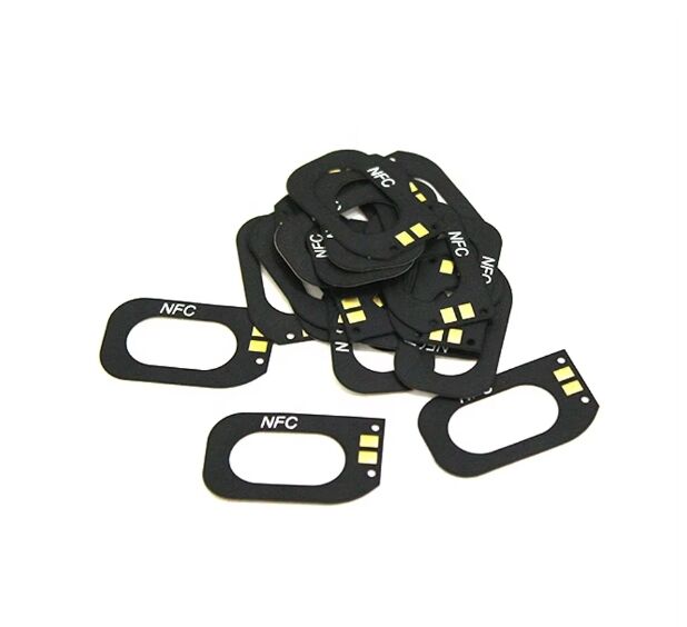
You can find NFC antenna PCBs in a lot of devices you interact with daily, including smartphones, tablets and smartwatches. These antennas are meticulously installed in the devices during manufacturing to ensure that they perform well. It's faster and more convenient than wireless, and Using NFC adds an extra level of safety to devices.
NFC antenna PCBs need to be designed and manufactured carefully to ensure that they work well. Clever engineers labor to make these antennas work better, so that devices connect more seamlessly. By optimising design and choice of materials, they guarantee fast, reliable communication with NFC antenna PCBs.
Today, the functions and advantages of NFC antenna PCB technology have helped to simplify our lives and make things more convenient. NFC antennas enable fast sharing files & make contactless payments safe and easy, even with a touch. These are antennas that take our world to another level of connection with the devices they serve.
Can offer simulation service HFSS software. HFSS software provide simulation service.lt declared a "high technological enterprise province Shanghai nfc antenna pcb"
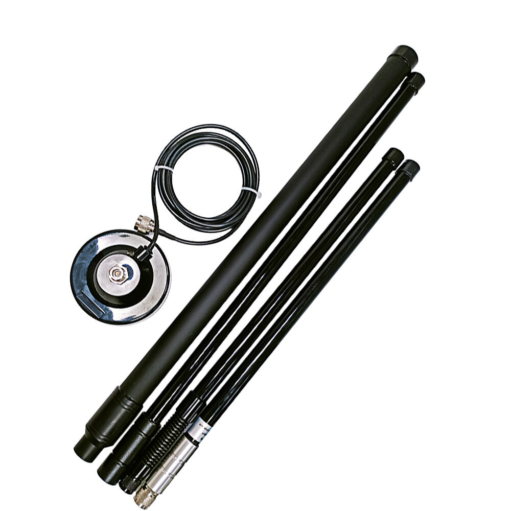
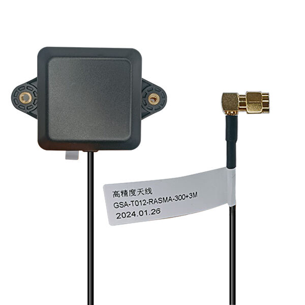
nfc antenna pcb 20 structural engineers well as engineers RF 285 production personnel 10,000 SM factory. Company 62 patents communications antennas as well GPS antennas. 100 countries areas served.
Signal Plus nfc antenna pcb years manufacturing experience LTE antenna,GPS antenna industry.Annual shipment quantity reaches 20,000,000 antenna units.Company 450+employees production 20 Lines meet customers'requirements full terms.
Signal Plus Technology Co, Ltd is nfc antenna pcb producer an antenna 2G/3G/4G/5G capabilities, WIFl antenna, Lora antenna GPS antennas, FPC/PCB antennas Combo antenna, Fiberglass antenna etc. With 9000 square meters facility, a highly skilled RD team, Signal Plus Technology Co. Ltd established the year 2015.

 EN
EN
 ES
ES
 PT
PT
 NL
NL
 AR
AR
 HR
HR
 CS
CS
 DA
DA
 FI
FI
 FR
FR
 DE
DE
 EL
EL
 IT
IT
 JA
JA
 KO
KO
 NO
NO
 PL
PL
 RO
RO
 RU
RU
 SV
SV
 TL
TL
 IW
IW
 ID
ID
 LT
LT
 SR
SR
 SK
SK
 SL
SL
 UK
UK
 VI
VI
 ET
ET
 HU
HU
 MT
MT
 TH
TH
 TR
TR
 FA
FA
 GA
GA
 BE
BE
 IS
IS
 LB
LB
 BG
BG