
 EN
EN
 ES
ES
 PT
PT
 NL
NL
 AR
AR
 HR
HR
 CS
CS
 DA
DA
 FI
FI
 FR
FR
 DE
DE
 EL
EL
 IT
IT
 JA
JA
 KO
KO
 NO
NO
 PL
PL
 RO
RO
 RU
RU
 SV
SV
 TL
TL
 IW
IW
 ID
ID
 LT
LT
 SR
SR
 SK
SK
 SL
SL
 UK
UK
 VI
VI
 ET
ET
 HU
HU
 MT
MT
 TH
TH
 TR
TR
 FA
FA
 GA
GA
 BE
BE
 IS
IS
 LB
LB
 BG
BG
/images/share.png)
It is always crucial to take into account the location of the PCB antenna on the board while designing electronic equipment. Through PCB antenna layout, the transmitted and received signals by the device are made sure to be controllable and not distorted. In this article, we will understand why the PCB antenna layout needs to be optimized for good signals and give some handy tips to improve the signal quality as well.
Importance of PCB Antenna Design for Distortion-Free Signals
PCB antenna design is very important as it delivers signals between the components of devices without any issue. Antenna designs offer much less in terms of signal distortion and noise, thus making devices more efficient. Careful design of the location of the antenna on the PCB will enable designers to have strong signals and the device perform as desired.
Improving Signals through Placing PCB Antennas: Tips
Therefore, certain considerations should be brought into play in placing the PCB antenna on the board to enhance signal performance. Take note of the board's layout initially and place the antenna in an area that won't interfere with other components. Besides, it is important to place the antenna at a distance from potential interference sources such as power supplies and high-speed digital circuits. To improve this and hence make the device more dependable, the designers can focus on choosing the location of the antenna carefully and minimizing interference.
With regard to the PCB Antennas for Firm signals on the PCB
There are certain things that designers should keep in mind in order to receive a good signal through bluetooth pcb antenna. One of the most important things is how long and how well the traces are connected between circuitry and antenna. Poor design may carry a full signal, but traces as specified maintain it just right. Designers also require a ground plane on the PCB to reduce noise and cross-talk, enhancing signal quality.
PCB Antenna Signal Quality and its Layout Impact
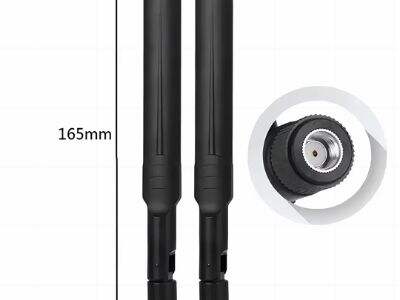
2.4 ghz pcb antenna layout design is a significant contributor to signal quality. Incompetent layout can lead to signal noise, distortion, and interference, restricting the device performance. Through optimizing the male sma connector and minimizing interference, designers ensure proper signal transmission and reception. By taking into account the factors that influence signal quality, designers can guarantee robust signals in printed circuit board (PCB) antennas and also optimize the performance of the device.
PCB Antenna Design for Maximum Signal Quality
Good male rf coaxial connector enables the designers to have various approaches that they can use to provide good signal quality. With any of those techniques, one can have the best antenna location for a more accurate, more reliable signal. Designers improve the quality and reliability of the signal by moving the antenna to a location where such issues are avoided. The use of ground planes and well-designed traces also improves signal quality through signal reduction in loss and distortion. Applying these practices during the design phase, the designers are able to improve this PCB antenna layout for a strong signal as well as improve the overall product performance.
Finally, the rf connector modification is essential to the improvement of the signal and the correct functioning of the electronic devices. Designers may improve signal quality and reliability by understanding the effect of PCB antenna layout on signal quality, guidelines for better placement, design factors, ways the layout will influence signals, and how to obtain great signal quality. Designers may improve signal quality and device performance by sustaining this during the design phase and paying attention to these aforementioned areas.