
 EN
EN
 ES
ES
 PT
PT
 NL
NL
 AR
AR
 HR
HR
 CS
CS
 DA
DA
 FI
FI
 FR
FR
 DE
DE
 EL
EL
 IT
IT
 JA
JA
 KO
KO
 NO
NO
 PL
PL
 RO
RO
 RU
RU
 SV
SV
 TL
TL
 IW
IW
 ID
ID
 LT
LT
 SR
SR
 SK
SK
 SL
SL
 UK
UK
 VI
VI
 ET
ET
 HU
HU
 MT
MT
 TH
TH
 TR
TR
 FA
FA
 GA
GA
 BE
BE
 IS
IS
 LB
LB
 BG
BG
/images/share.png)
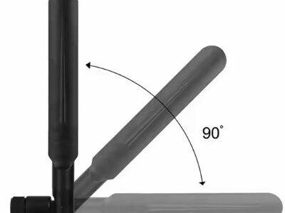
When we use our electronic devices — smartphones, tablets, and laptops — to browse the internet or communicate with others wirelessly, we rely on a PCB antenna. PCB antenna is a specific type of antenna that can be manufactured directly on a PCB (printed circuit board). It allows our devices to send and receive signals without wires.
Impact of PCB Antenna Design on Signal Strength
Depending on how a PCB antenna is designed, it may alter the communication of our devices with Wi-Fi, Bluetooth, and other wireless networks. Certain designs can boost the signal, implying our devices retain contact even when we are wayaway from the wireless source. Other designs can let our devices communicate over longer distances, so we can stay connected in larger spaces like schools or playgrounds.
What is PCB Antenna and how to optimize the performance?
The PCB antenna to be made is not enough, you also need to consider the placement location on the circuit board. When a PCB antenna is near other electronic components or metals, it can even confuse the signal and weaken the connection. But if the PCB antenna is placed in an open space without obstruction, it can be more effective, and play a role in making our devices connect properly with defined features.
Good design choices for making wireless connections stronger
In order to keep our devices connected under varying circumstances, engineers select specific types of PCB antenna and locations on the circuit board. The most appropriate rf connectors and arrangement can ensure wireless connectivity is perfect, it allows our devices to receive and transmit signals continuously. Not only that smart PCB antennas design is making our devices less prone to failures but also easy-to-use.
Interference and Signal Loss Problems & Solutions
One major problem in the world of wireless communication is interference or the disruption of the signals sent and received by our devices. Engineers can further minimize signal loss and ensure good connectivity in our devices by using advanced PCB antenna designs that can withstand interference. The use of rf cable is an innovative solution to ensure that we can handle with interference and loss at long distance wireless communication, to guarantee we can always work and connect anywhere we go.
Conclusion PCB antenna design is significance of enhancing the wireless communication of our electronic devices. So, by comprehending principles of PCB antenna, analyzing factors affecting the gain and range of PCB antennas, optimizing placement of PCB antennas, implementing efficient design techniques and troubleshooting interference issues we can ensure robust communication of our devices. Proper PCB mixed signal antenna designs allow our devices to keep us connected, in an increasingly wireless world.