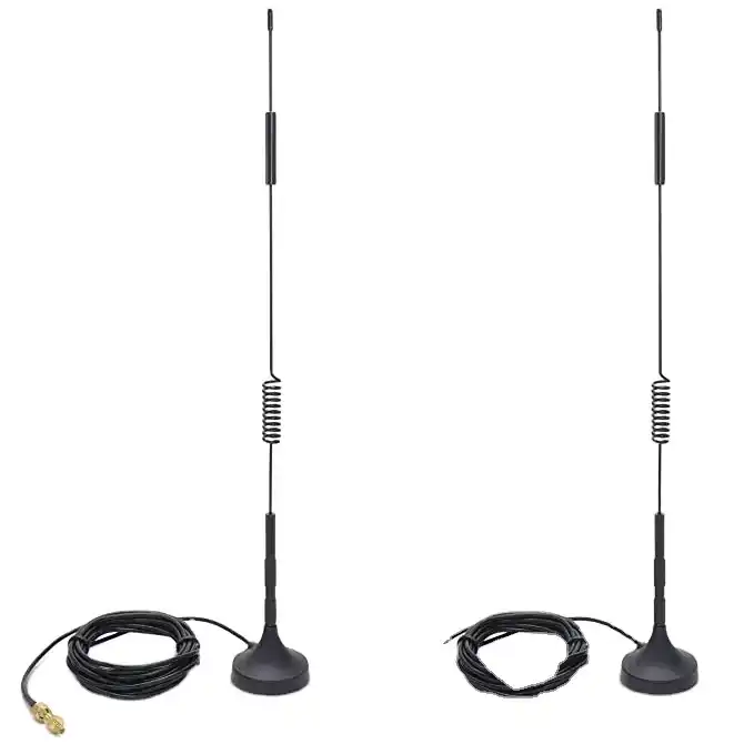
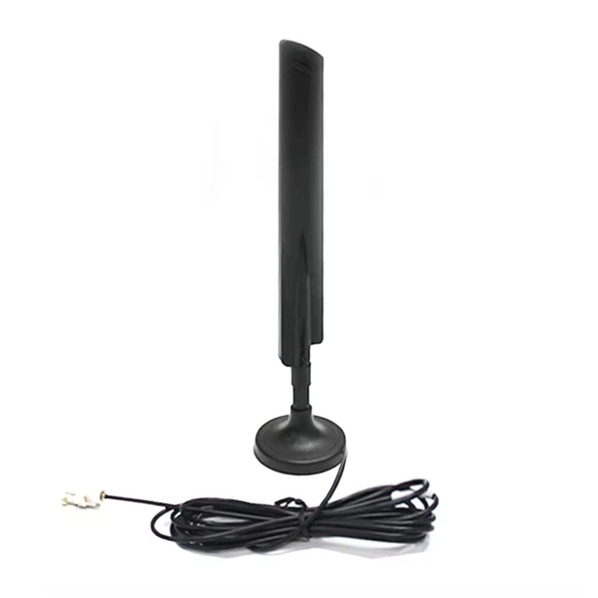
It is that one small component in the world of mobile technology we never think about until it stops working and that is our GSM antenna PCB – and it is small and powerful. This little circuit board receives signals from cell towers and sends those signals to our phones, enabling us to make calls, send texts and surf the internet.
Jun 14 At the heart of our concerns for getting good signal reception on our mobile devices is the GSM antenna PCB. A quality PCB can ensure our phones get strong signals, even in dead spots with no network at all. On the contrary, a bad design of PCB can cause dropped calls, slow ireless or internet speed and frustration to end user.
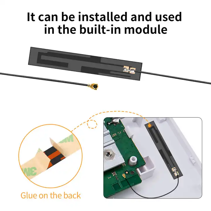
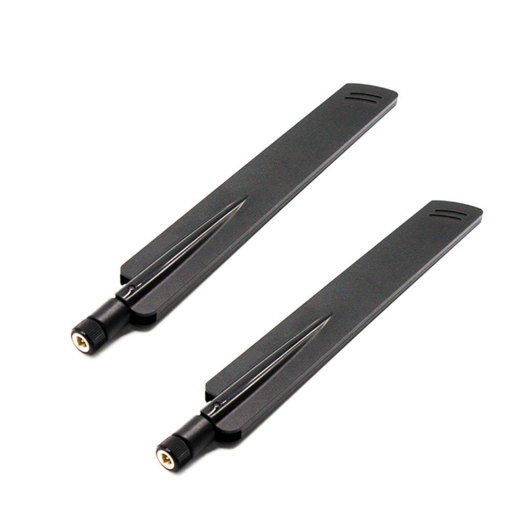
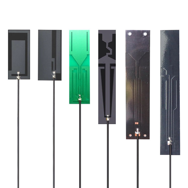
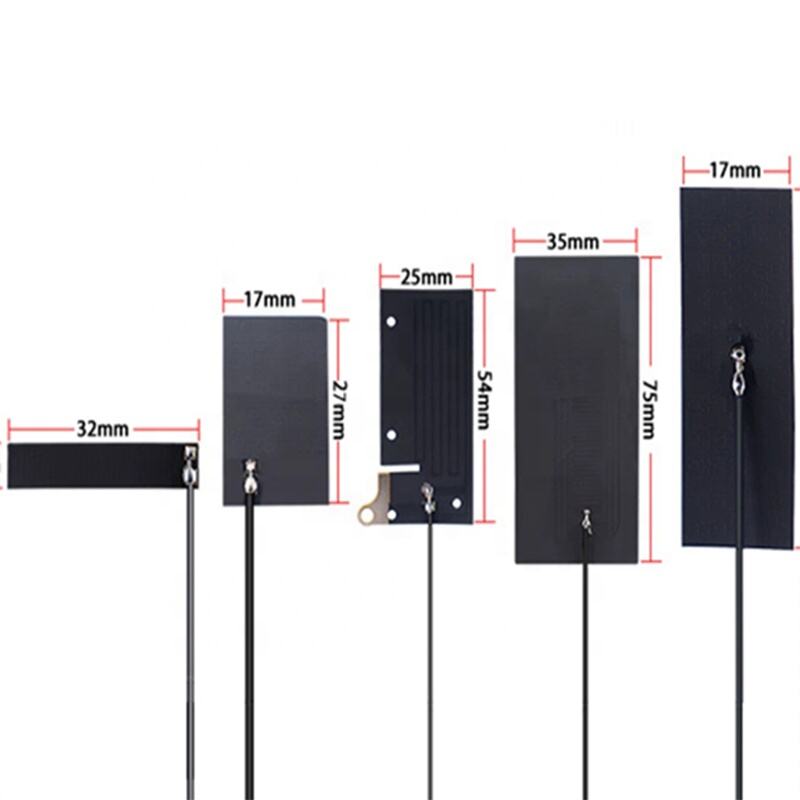
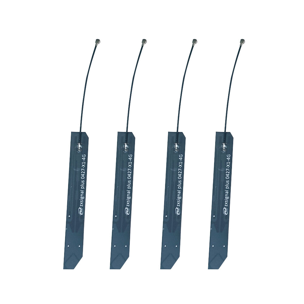
There are a number of different types of GSM antenna PCBs and configurations that are found in wireless devices. Some devices are provided with one PCB for both the GSM antenna and other RF functions, and some devices are provided with separate PCBs for the antenna and the other functions. The positioning and architecture of the PCB could affect the signal strength and performance of the system.
To maximize the performance of the GSM antenna PCB, its placement in the mobile becomes important. The PCB can be placed in a place that may receive the best signal and away from other things that will affect its performance. And with the PCB being well positioned, manufacturers are able to guarantee a strong signal and reliable connectivity for users.
Due to their small size, GSM antenna PCBs may occasionally suffer problems which affect their connectivity. Typical problems include bad connections, burned-out components, or signal snarled by another electronic gadget. By addressing such concerns and having the PCB fixed or replaced if needed, you get to take advantage of better connectivity and overall mobile experience.
Signal gsm antenna pcb 10 years manufacturing experience LTE antenna, GPS antenna industry. Annual shipment quantity reaches 20,000,000 antenna units. Company 450+employees production 20 Lines meet customers' requirements full terms.
gsm antenna pcb 20 structural engineers Engineers RF 285 production personnel 10,000 SM factory. 62 patents communications antennas GPS antennas. than 100 countries regions are served.
Signal Plus Technology Co, Ltd. is top provider antennas 2G/3G/4G/5G, WIFlantenna, Lora, GPS, FPC/PCB, Combo, Fiberglass, Since gsm antenna pcb 2015, it a 9000 square meters manufacturing space an experienced team of RD.
Can offer simulation service HFSS software. HFSS software provide simulation service.lt declared a "high technological enterprise province Shanghai gsm antenna pcb"

 EN
EN
 ES
ES
 PT
PT
 NL
NL
 AR
AR
 HR
HR
 CS
CS
 DA
DA
 FI
FI
 FR
FR
 DE
DE
 EL
EL
 IT
IT
 JA
JA
 KO
KO
 NO
NO
 PL
PL
 RO
RO
 RU
RU
 SV
SV
 TL
TL
 IW
IW
 ID
ID
 LT
LT
 SR
SR
 SK
SK
 SL
SL
 UK
UK
 VI
VI
 ET
ET
 HU
HU
 MT
MT
 TH
TH
 TR
TR
 FA
FA
 GA
GA
 BE
BE
 IS
IS
 LB
LB
 BG
BG